SoC Integration
片上系统集成
This section describes the functional details of NANHU top-level interfaces.
It's worth noting these are the typical configurations and the user may specify different architecture parameters.
本章节介绍南湖顶层接口的功能细节。
值得注意的是,这些是典型配置,用户也可以指定不同的架构参数。
Clock and Reset 时钟与复位
NANHU has two clock domains:
南湖有两个时钟域:
-
One clock domain for the cpu core (
io_clock). All clock in CPU core isio_clock.
处理器核时钟域(io_clock)。处理器核中的所有时钟都是io_clock。 -
One clock domain for jtag (
io_systemjtag_jtag_TCK).
JTAG时钟域(io_systemjtag_jtag_TCK)。
NANHU has the following reset signals.
All Reset signals are Asynchronous Resets.
南湖有以下复位信号。
所有复位信号均为异步复位。
-
io_resetis internally synced with the clockio_clock. Active high.dio_reset在内部与时钟io_clock同步。 高电平有效。 -
io_systemjtag_resetis internally synced with the clockio_systemjtag_jtag_TCK. Active high.io_systemjtag_reset在内部与时钟io_systemjtag_jtag_TCK同步。 高电平有效。
There are two types of synchronizers in the RTL. All instances are used to synchronize the reset.
RTL 中有两种类型的同步器。 所有实例均用于同步重置。
-
AsyncResetSynchronizerPrimitiveShiftReg(synchronize reset fromjtag_clocktoio_clock, from low frequency to high frequency)AsyncResetSynchronizerPrimitiveShiftReg(从jtag_clock同步复位到io_clock,从低频到高频) -
ResetGen/ResetGenDFT(used to synchronize for bothjtag_clockandio_clock, depending on the instantiations)ResetGen/ResetGenDFT(用于同步jtag_clock和io_clock,取决于实例化)
AXI Interface AXI总线接口
For our definitions of the three ports,
以下是南湖中三个AXI总线接口的定义。
- 256-bit AXI Memory Port: for CPU to access DDR (CPU is the master)
256位AXI内存端口:供CPU访问DDR(CPU为主设备)
Address space: DDR space (0x8000_0000 to 0xf_ffff_ffff)
地址空间:DDR空间(0x8000_0000到0xf_ffff_ffff)
AXI ID width: 6-bit
AXI ID 位宽:6 位
Number of outstanding transactions: 56 (max. supported by L3 cache)
未完成事务数:56(最大值。由L3缓存支持)
Max transaction size: 64 bytes
最大事务大小:64字节
Number of IDs: 64
ID数量:64
Max number of outstanding transactions per ID: 1 每个ID的最大未完成事务数:1
- 64-bit AXI Peripheral Port: for CPU to access peripherals (CPU is the master)
64位AXI外设端口:供CPU访问外设(CPU为主设备)
Address space: peripheral slaves space (0x0000_0000 to 0x7fff_ffff)
地址空间:外设从机空间(0x0000_0000至0x7fff_ffff)
AXI ID width: 2-bit
AXI ID 位宽:2位
Number of outstanding: 1 for instruction and 1 for data for each core
未完成事务数量:每核1条指令,1条数据
Max transaction size: 8 bytes
最大事务大小:8字节
Number of IDs: 4 (though the ID is 4-bit, most of them are not used)
ID数量:4个(虽然ID为4位,但大部分没有被用到)
Max number of outstanding transactions per ID: 1
每个ID的最大未完成事务数:1
- 256-bit AXI DMA Port: for peripherals to access CPU/DDR (CPU is the slave)
256位AXI DMA端口:供外设访问CPU/DDR(CPU为从设备)
Address space: DDR space (0x8000_0000 to 0xf_ffff_ffff)
地址空间:DDR空间(0x8000_0000至0xf_ffff_ffff)
AXI ID width: 8-bit
AXI ID位宽:8 位
Number of outstanding supported by CPU: 32
CPU支持的未完成事务数:32
Different transaction sizes and transactions per ID are supported. They are changed into 256-bit TileLink transactions internally. One AXI transaction may be split into multiple TileLink transactions.
AXI接口支持不同事务大小和每个ID的事务。它们在内部被转换为256位TileLink 事务。一个AXI事务可以被拆分为多个TileLink事务。
This DMA port allows the peripherals to access DDR under coherency with the CPU caches. They can send standard AXI aw/w/ar requests to this port to write/read the DDR. Memory coherency is supported in the DMA port by the L3 cache. No explicit action is needed to sync the data with CPU.
DMA端口允许外设在CPU缓存一致时访问DDR。它们可以向此端口发送标准AXI aw/w/ar请求以写/读DDR。DMA 端口中的内存一致性由L3缓存保证。数据与CPU的同步不需要显式操作。
Note: RISC-V defines a weak memory order. Load and store instructions are not required to be visible to other harts (CPU cores, DMA devices, etc) before an explicit memory barrier instruction like fence. For example, in NANHU, data in store queue and committed store buffer is not under coherency with the
CPU caches. To read newly stored data through DMA AXI port, a fence instruction must be used in software to make the CPU stores visible to the coherent cache hierarchy. This is a RISC-V requirement, not a bug/issue of NANHU.
请注意:RISC-V定义了弱内存序。在fence等显式内存栅障指令之前,load和store指令不需要对其他硬件线程(CPU内核、DMA设备等)可见。例如,在南湖中,存储队列和提交存储缓冲中的数据与CPU缓存不具有一致性。为了通过DMA AXI 端口读取新存储的数据,必须在软件中使用栅障指令以使CPU存储对一致的缓存层次结构可见。这是RISC-V的要求,而不是南湖的错误/问题。
Memory Map 内存映射
There are three main regions:
内存映射有三个主要区域:
-
Peripheral slaves space 0x0000_0000 to 0x7fff_ffff
外设从设备空间(0x0000_0000 to 0x7fff_ffff) -
DDR space: 0x8000_0000 to 0xf_ffff_ffff
DDR空间(0x8000_0000 to 0xf_ffff_ffff) -
DMA to access DDR: 0x8000_0000 to 0xf_ffff_ffff
用于访问DDR的DMA(0x8000_0000 to 0xf_ffff_ffff)
Peripherals in the Peripheral address space is mostly determined by the SoC.
外设地址空间中的外设大部分由SoC确定。
Default PMA is configured according to NANHU mamory map. Illegal memory access will cause access fault exceptions.
Please remember to update the default PMA settings if you need to change the peripheral address mappings.
默认PMA根据南湖内存映射配置。 非法的内存访问将导致访问错误例外。如果您需要更改外设地址映射,请务必更新默认PMA设置。
Internal peripheral address space:
以下是内部外设地址空间:
| Device | Start Address | End Address |
|---|---|---|
| CLINT | 0x3800_0000 | 0x3800_ffff |
| BEU | 0x3801_0000 | 0x3801_ffff |
| Debug Module | 0x3802_0000 | 0x3802_0fff |
| L3CacheCtrl | 0x3900_0000 | 0x3900_0fff |
| PLIC | 0x3c00_0000 | 0x3fff_ffff |
Real-Time Clock (CLINT) 实时时钟
By default, the real-time clock in NANHU operates at 1/100 frequency of the CPU clock io_clock.
默认情况下,南湖中的实时时钟频率为CPU时钟io_clock频率的1/100。
It can be optionally configured with an external real-time clock input io_rtc_clock. This clock usually operates at a fixed frequency ranging between 1MHz ~ 100MHz. The frequency is implementation defined and used by software in device tree. Example is shown in the southlake branch.
该时钟可以选择性地配置一个外部实时时钟输入io_rtc_clock。该时钟通常在 1MHz ~ 100MHz之间的固定频率下工作。频率由设备树中的软件定义和使用。 软件示例在southlake分支中。
Interrupt 中断
There are local (CLINT) and global (PLIC) interrupt controllers available with NANHU core.
The PLIC and CLINT as shown in the below figure are for dual-core configuration.
南湖核心提供本地 (CLINT)和全局 (PLIC)的中断控制器。
下图所示的PLIC和CLINT适用于双核配置。
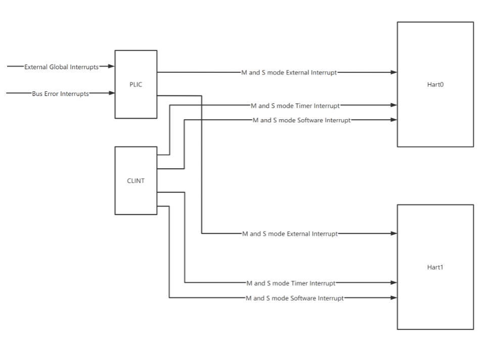
Local interrupt sources in NANHU includes timer interrupt and software interrupt.
All the local interrupts are generated by CLINT for S-mode and M-mode.
南湖中的本地中断源包括定时器中断和软件中断。
S模式和M模式的所有本地中断均由CLINT生成。
Global interrupt controller follows the RISC-V Platform-Level Interrupt Controller Specification.
PLIC is connected via 64-bit TileLink.
全局中断控制器遵循RISC-V平台级中断控制器规范。
PLIC通过64位TileLink 连接。
Below is the interrupt number mapping in PLIC.
Interrupt 0 is always reserved by the PLIC.
以下是PLIC中的中断号映射。
0号中断始终由PLIC保留。
| Interrupt No. | name | description |
|---|---|---|
| 0 | Reserved 保留 |
- |
| 1~64 | external interrupt 外部中断 |
From top-level io_extIntrs 来自顶层的io_extIntrs |
| 65 | bus error interrupt 0 总线故障中断0 |
Core 0 bus error interrupt 0号核总线故障中断 |
| 66 | bus error interrupt 1 总线故障中断1 |
Core 1 bus error interrupt 1号核总线故障中断 |
The global interrupt sources in NANHU includes external global interrupts and bus error interrupts.
External global interrupts are generated by external devices.
The bus error interrupts are generated by CPU hart0 and hart1.
南湖的全局中断源包括外部全局中断和总线故障中断。
外部全局中断由外部设备生成。
总线故障中断由CPU hart0和hart1生成。
Debug 调试
NANHU implements RISC-V External Debug Support Version 0.13.2.
南湖实现了RISC-V外部调试支持0.13.2版本。
Wait for Interrupt (WFI) 等待中断
By default, NANHU implements WFI as NOP.
南湖默认将WFI实现为NOP。
It can be optionally configured to behave as the real wait-for-interrupt. Example is shown in the southlake branch.
它可以被手动配置为真正的等待中断。示例在southlake分支中显示。
However, it's worth noting the software must handle the case WFI is treated as NOP or WFI returns without a taken interrupt, even if NANHU is configured with the real wait-for-interrupt mode.
然而,值得注意的是,即使南湖配置了真正的等待中断模式,软件也必须处理WFI被视作NOP或WFI返回而没有发生中断。
You can refer to the RISC-V privledge manual for more information in Section 3.3.3 (Wait for Interrupt). We cite some requirements below.
您可以参阅RISC-V权限手册的第3.3.3节(Wait for Interrupt)以获取更多信息。我们在下面引用一些要求。
If the event that causes the hart to resume execution does not cause an interrupt to be taken, execution will resume at pc + 4, and software must determine what action to take, including looping back to repeat the WFI if there was no actionable event.
如果导致硬件线程恢复执行的事件不会导致中断发生,执行将在pc + 4处恢复,同时软件必须确定要采取的操作,包括在没有可操作事件时循环返回以重复 WFI。As implementations are free to implement WFI as a NOP, software must explicitly check for any relevant pending but disabled interrupts in the code following an WFI, and should loop back to the WFI if no suitable interrupt was detected.
由于可以自由将WFI实现为NOP,软件必须显式地检查WFI后面的代码中任何相关的待处理但已禁用的中断,并且在未检测到合适的中断时循环返回到 WFI。